

Photovoltaic solar energy is the leader in the evolution of electricity mixes taking us away from fossil fuels. Why and how has it acquired this position? The answer is to be found first and foremost in the progress of its technology.
To understand the place photovoltaic solar energy has made for itself in electricity mixes, it is essential to know the resource and principles of converting solar radiation into heat or electricity. (Read: Énergie solaire : les bases théoriques pour la comprendre), but it is also necessary to discover its origin and the trajectory of the main technologies that convert solar radiation. After those that ensure the production of heat for domestic or industrial purposes (Read: Solaire thermique : les technologies et leurs trajectoires), come those that allow direct electricity generation.
Born in the early 1950s, photovoltaic technologies took off industrially in Japan and then in the United States in the 1980s with the production of high-efficiency crystalline silicon-based cells (Read: Solaire thermique et photovoltaïque : une brève histoire). Since then, their large-scale production and reduced costs have been achieved through the technological development of materials and the manufacture of photovoltaic cells and modules.
1. Semiconductor materials
Photovoltaic collectors are mainly distinguished by the nature of the semiconductor materials used, whose choice is dictated primarily by physical principles and in particular the adaptation of the bandgap width to the solar spectrum (Read: Énergie solaire : les bases théoriques pour la comprendre).
But the choice is also largely dictated by practical considerations: availability of the material, ability to produce it with the required crystalline quality and purity at an acceptable cost, possibility of making a junction without difficulty, feasability of making ohmic contacts of low resistance.
Crystalline silicon quickly became the first choice for several reasons:
- it is the only elementary semiconductor (consisting of a single atom) to have a suitable band gap
- after oxygen, it is the most abundant on the earth’s crust
- we are capable of producing high quality crystals and can benefit from all the efforts made in the microelectronics industry
In return for these advantages, silicon has a serious disadvantage: as it does not absorb infrared photons well, it is necessary to use fairly thick crystals (more than 70 mm) to minimize loss in conversion efficiency, which forces an overkill in quality and does not go in the direction of minimizing costs [1].
Another consequence of this high thickness is the relative complexity of implementation with the slicing of the large crystals into wafers, the manufacturing of cells on these individual wafers and finally the assembly of these cells to connect them together in modules.
These drawbacks have led to the development of other materials, mainly compound semiconductors (several atoms in their composition) that can be used in very thin layers. They are most often deposited on a glass substrate. Thicknesses vary according to the material, from a few hundred nm to a few mm. These layers are then structured to isolate and connect cells in series, but at the scale of the entire glass plate.
Three materials are used commercially and take up the market share left by silicon: cadmium telluride (CdTe), chalcopyrites such as Cu(In,Ga)Se2 (CIGS) and hydrogenated amorphous silicon.
Although hydrogenated amorphous silicon is made of silicon, it does not have the same structure and therefore not at all the same electronic band structure, which allows it to be used in very thin layers (400 nm).
A last emerging family is that of organic materials. In some organic materials called Pi conjugates, it is also possible to have electron levels such that one can induce electron transitions from one band to another and thus obtain an electron conduction induced by photo-generation, i.e. passage of electrons in the upper band after photo-excitation. These materials have two essential qualities: an ability to absorb the solar spectrum with very low thicknesses and the possibility of being implemented by very cheap printing techniques.
2. Manufacturing methods for photovoltaic cells and modules
They differ according to the semiconductor materials used.
2.1. Cells using crystalline silicon
Silicon is the basis of the most important photovoltaic industry. The manufacturing technology for the modules that use it is complex (Figure 1).
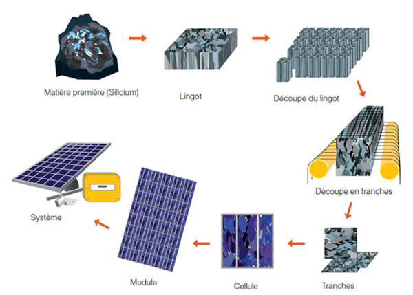
The process goes from the raw material obtained by carbo-reduction of quartz to the final module, this through refining, crystallization, cutting into wafers, manufacturing of cells and assembly into modules.
2.1.1. The silicon material
Silicon is obtained from quartz ore or silica (SiO2) which is a basic constituent of primary rocks, the majority of rocks being silicates. It is extracted by carbo-reduction, a high-temperature reaction between quartz and carbon:
SiO2(s) + 2 C(s) ==> Si(l) + 2 CO(g)
This is usually done using charcoal that is purer than hard coal.
Temperatures for this reaction are close to 2000°C. Heating is done using carbon bars as resistors, into which very strong electric currents are injected: in reality, they are a consumable because they participate in the reaction.
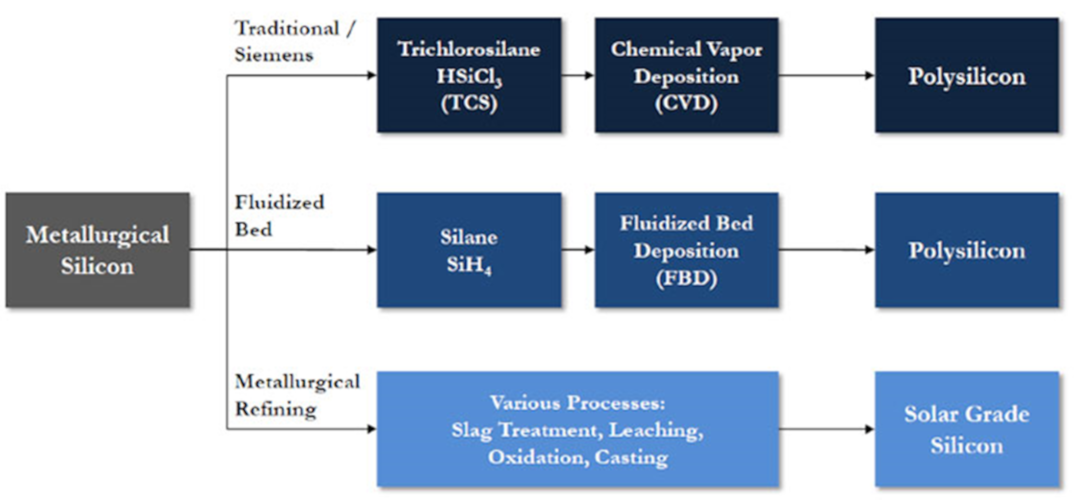
The liquid silicon thus obtained flows out of the furnace and, as it cools, it crystallizes. At this stage it contains about 1% impurities. If it is used as it is and in large quantities in the polymer industry (silicone) and the metallurgy industry (additive for aluminum in automobile engines), it is much too impure for the microelectronics or photovoltaic industries (Figure 2). It is therefore purified essentially using three methods, the first two of which consist of obtaining a gas (Tri-Chloro-Silane or TCS: SiHCl3 or Silane: SiH4). To do this, solid silicon is reacted with chlorine (Cl2) or hydrogen (H2).
The silicon is reacted again by decomposing the molecule by thermal activation in furnaces (chemical vapor deposition).
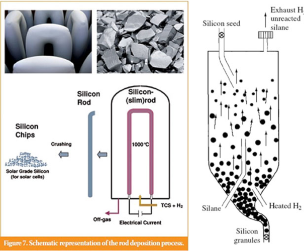
For chlorosilane SiHCl3, resistive furnaces are used by heating silicon rods on which the silicon is deposited (“Siemens” process), which is the most common process. For SiH4 silane, fluidized bed furnaces are used, with the silicon condensing and forming powders in the gas stream that is recovered at the outlet (Figure 3).
A final purification method that is not widely used is to keep the silicon in the solid or liquid phase and to carry out various treatments, either chemical or melting/crystallization: in this case, the effect of segregation of impurities between the two phases during crystallization is used. These purification processes are known as metallurgical.
But the silicon thus obtained – if it is very pure, with impurity levels approaching the part per billion -ppb (10-9) – is not yet suitable to make a good cell, because as we have seen in the principles article, it must have a crystal structure (arrangement of atoms) close to that of monocrystals.
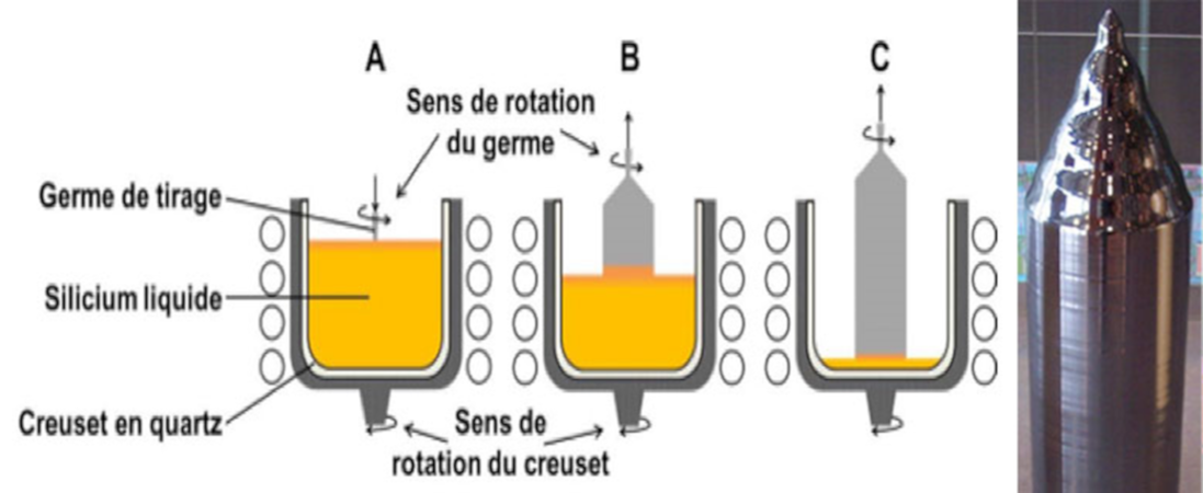
The next step is therefore to melt it and crystallize it again under special conditions. For photovoltaics, there are essentially two methods used.
- Single crystal pulling, by the Czochralski method, consists of melting silicon in a silica crucible, dipping a rotating single crystal seed in the bath, and finally controlling the temperature gradients in the bath and the upward movement of the seed, gradually crystallizing the silicon from the seed, taking care to increase the diameter of the crystal. Rotation of the seed and crucible results in a perfectly monocrystalline, long, cylindrical rod without dislocations, with a diameter of about 20 cm and a length of several meters (Figure 4).
- Very coarse-grained polycrystal can be pulled by the technique of directed solidification (Figure 5). As before, the silicon is melted in a large, parallelepiped-shaped crucible (typically 1 meter sideways and 50 cm high); the system is then cooled by extracting heat from the bottom of the crucible so that the silicon solidifies from the bottom. Crystalline nuclei appear at the bottom of the crucible. From these nuclei, a so-called columnar growth is obtained with an increase in grain size as the solid-liquid front spreads (Figure 5). The grain size is typically of the order of 1 cm2 of the section at the top of the ingot, once the silicon has completely crystallized. To obtain the best possible quality, a solid-liquid interface should be maintained as flat as possible. For this second technique, we speak of poly – or multicrystalline silicon.
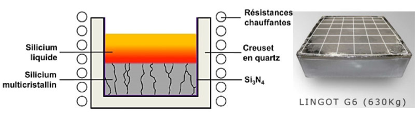
While the cost of silicon crystals obtained by this second method is lower than that of monocrystals obtained by the first, the crystal quality, and hence the yield of the cells, is also lower.
In both cases, a small quantity of an impurity known as dopant is added, either boron to obtain a p-type semiconductor (conducting through excess holes), or phosphorus to obtain an n-type material (conducting through excess electrons).
Once obtained, these large crystals are first cut into parallelepipedal bars of the order of 125 to 150 mm in length. In the case of single crystals pulled by the Czochralski method, the cylinder is partially trimmed to obtain a section that is not perfectly square but close to square (called pseudo-square).
These bars are then cut into very thin slices of 150 to 200 mm thick using wire saws, diamond wires or simple moving wires in a liquid charged with very fine abrasive particles.
2.1.2. The manufacture of silicon-based cells
It is on these thin slices that the cells will then be made. In particular, the junction and the contact is made using metal electrodes. In the case of the most common cells, made of p-type material, there are, by production sequence, different elements on each side (Figure 6).
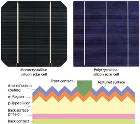
On the front side:
- an n-type doped zone, obtained by diffusion of phosphorus at high temperature and over a certain thickness, which makes it possible to obtain the n/p junction
- a plasma-enhanced chemical vapor deposition (PECVD) silicon nitride layer which serves as an anti-reflection layer
- a metallization carried out by screen-printing in the form of thin fingers and bus-bar, which makes it possible to come into contact with the silicon after an appropriate heating step; this metallization consists of a silver paste
On the back side, there is a paste-based metallization deposited by screen-printing over the entire surface: this silver-based paste contains a little aluminum, which during subsequent heat treatments diffuses into the silicon and thus reinforces the p-doping locally. It thus makes it possible to create an electric field that repels the photo-generated electrons towards the front side (Back Surface Field concept).
Prior to the above processes, silicon is chemically etched in a strong base or a mixture of strong acids to dissolve the silicon on the surface, thus eliminating the area damaged by sawing and producing a specific texture on the surface. This reduces the reflection coefficient for incident radiation.
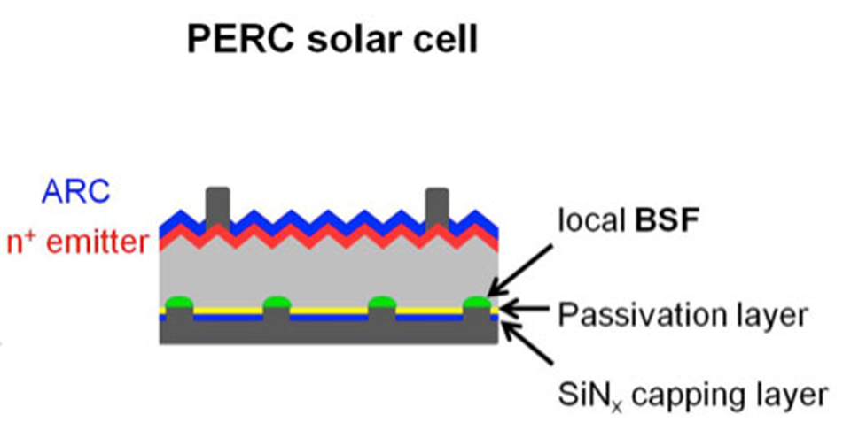
Numerous technological variants exist, or are being studied, which aim to increase the yield compared to this standard. For example, it is possible to maintain the p-type silicon and to cover the back side with a dielectric, leaving contact areas (Figure 7), which makes it possible to reduce the recombination of carriers on the back side: this is the concept of PERC (Passivated Emitter and Rear Cell) cells.
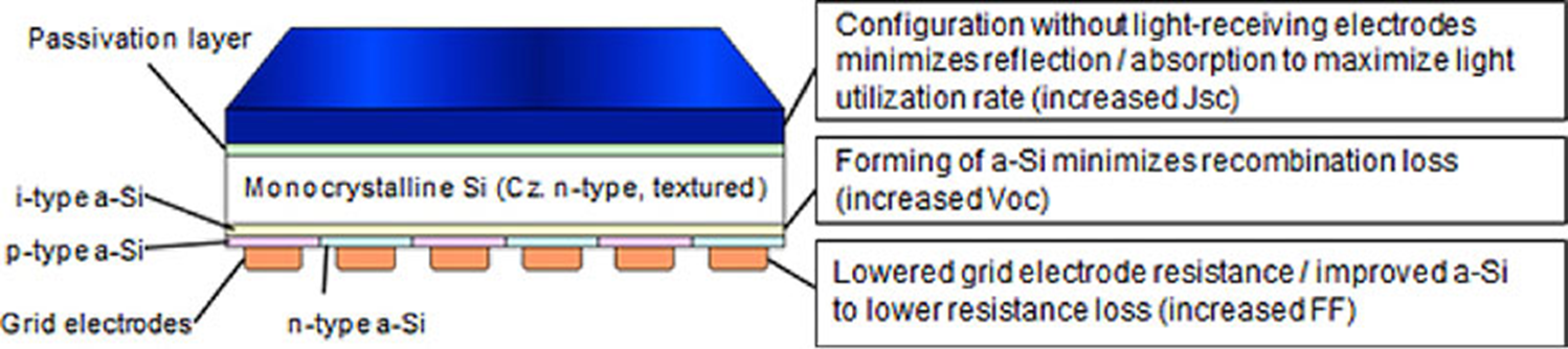
It is also possible to switch from silicon to n-type silicon, which is less sensitive to metallic impurities and allows particularly efficient surface passivation modes such as the use of hydrogenated amorphous silicon. These are known as heterojunction cells (HET or HJT). In this case, the junction is made between p-type hydrogenated amorphous silicon and n-type crystalline silicon, two materials with different electronic bands. This technology was commercially introduced in the 1990s by Sanyo of Japan.
Also on n-type silicon, both the emitter (p-type) and the base contact on the back side can be realized in a localized way according to an inter-digital finger structure. These are known as RCC (Rear Contact Cell) cells. This technique totally eliminates the presence of metal lines on the front panel and therefore completely eliminates shading on this panel. It was introduced by the American SunPower in the 2000s.
It is possible to combine inter-digital rear contacts and heterojunction (Figure 8), a combination which, to date, has made it possible to obtain the record yield in silicon (Panasonic-Sanyo) of 25.6%.
It is very important to keep in mind that these increasingly complex technologies are usually accompanied by additional costs. Industrial decisions are made according to criteria of economic relevance. There is therefore a strong gap between laboratory yields, which are initially not concerned with costs, and average production yields.
A higher efficiency cell can certainly be sold at a higher price because it will reduce the cost of other elements that enter into a system and, ultimately, reduce the cost per kWh, provided that the additional cost is not too high.
In addition, these new technologies lead to a change in the equipment stock, which implies delays (machine set-up time) and significant capital investment.
Nevertheless, there is a gradual shift from standard technology cells to so-called high-efficiency technologies (PERC, RCC, HJT and others).
2.1.3. Assembly of silicon cells for the manufacture of modules
Once produced, the silicon cells are assembled into modules that perform several functions:
- the series and parallel connection of the cells, in such a way as to cover a large surface area and to ensure a sufficiently high output voltage to avoid ohmic losses in the external circuits
- the protection of the cells and the internal connections against mechanical or chemical attack
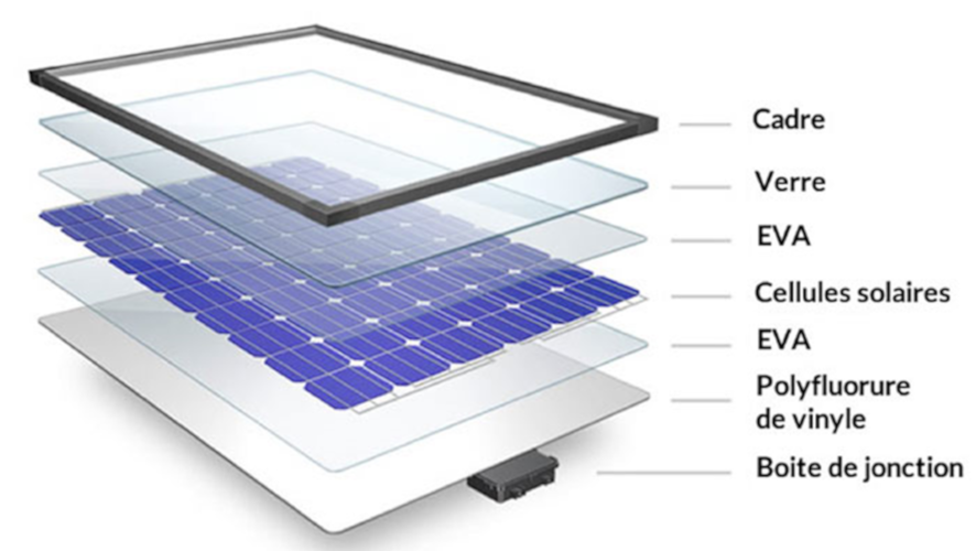
Typically, the usual modules have 60 or 72 cells of 150 mm side length each. They are about 1.5 m2 in size and deliver a power of 250 to 340 Wp at 24 V.
The module assembly consists of laminating together:
- a sheet of tempered glass on the front face
- a layer of cells previously connected together using tinned copper tapes (covered with a tin-based fusible material) and soldering these tapes to the cell busbars
- a material on the back side which may be either another glass plate or a sandwich of polymeric materials comprising at least one layer of fluoropolymer
- two intermediate layers of polymer to make the connection between the other three layers and to completely fill the intermediate volume where the cells and the copper ribbons are placed, these layers being called the encapsulants
All five stacked layers are then placed in a laminator for about ten minutes. Under uniform pressure, heating is carried out at temperatures of about 150°C for 10 minutes, which allows the encapsulants to flow, cross-link and expel bubbles.
A so-called junction box with bypass diodes is then placed on the rear side. Each of the by-pass diodes is associated with a sub-network of cells of the module. When the cells of the sub-array are shaded, the by-pass diode becomes conductive, i.e. the current flows through the diode, thus isolating the associated sub-array of cells from the electrical circuit. Without these diodes, the unlit cells would function as resistors and would heat up, which could lead to irreversible degradation.
Most often, as a final step, to ensure better mechanical strength and avoid subjecting the module to shocks and lateral chemical aggression, a peripheral aluminum frame is added, which is fixed to the module by Silicon type joints (Figure 9). This structure, which has changed little since the start of the photovoltaic industry, ensures a long service life for the modules provided that the rules of the trade are respected.
The modules are therefore guaranteed 20 to 25 years with a maximum degradation of less than 20%, i.e. 1% per year. They often continue to function beyond this period. The annual degradation rate varies from one module to another but is significantly below 1% per year.
2.2. Thin film cells and modules
The principle of manufacturing a thin-film photovoltaic module is completely different and in many ways much simpler (Figure 10). The semiconductor is directly deposited on a glass plate or polymer substrate. For this purpose, conventional deposition techniques are used, which are also used in other applications.
Four types of thin-film modules are currently available on the market using the following materials:
- CdTe (cadmium telluride) deposited by evaporation
- the chalcopyrites Cu(InxGa1-x)Se2 known as CIGS, deposited most often by cathodic sputtering: this is an alloy in which the proportion x can be varied between indium (In) and gallium (Ga)
- hydrogenated amorphous silicon Si(H)x or Si:H deposited by plasma-enhanced chemical vapour deposition (PECVD)
- conductive organic materials such as P-conjugated materials or organic perovskites deposited most often by printing techniques
Whatever the technology, the manufacturing principle is the same. A transparent conductive layer is first deposited on the substrate (glass or polymer), either locally if this layer is deposited by printing or over the entire surface. This is followed by local ablation, usually by LASER ablation techniques. This layer is intended to make contact on the semiconductor on the solar radiation entrance side.
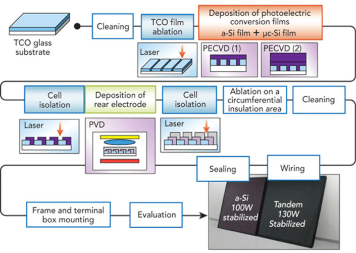
The active layers of the semiconductor junction must then be deposited where the photogeneration of carriers (holes and electrons) will occur. There are therefore at least two layers to create this junction. This sandwich of active layers is also deposited either locally or in a full layer, and then structured by localized ablation. Finally, a metallic conductive material is deposited in a thin layer that is also localized. The aim of these three successive depositions and structures is to create individual and strip-shaped photovoltaic cells and then to put them in series. This manufacturing principle can be visualized in the specific case of amorphous silicon/microcrystalline silicon tandem cells (Figure 10). A distinction is made between the individual layers and the way in which the cells produced in this way are arranged in series.
When examining the precise stacking of the individual cells such as CIGS , CdTe and hydrogenated amorphous silicon (Figure 11), a distinction is made between:
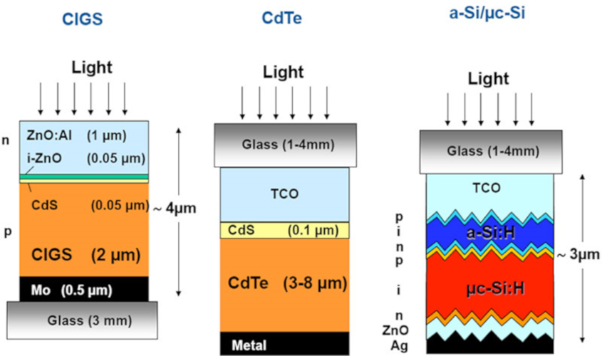
- the transparent conductive surface layer TCO (Transparent Conductive Oxide) most often based on layers of tin oxide or zinc oxide; these materials are in fact semiconductors with a wide band gap, therefore transparent for the solar spectrum, but naturally very conductive due to the presence of stoichiometric defects,
- for CdTe and CIGS, a layer of CdS used to create a heterojunction (Read: Énergie solaire : les bases théoriques pour la comprendre),
- the semiconductor layers themselves (the ones that serve as photo-absorbers),
- the metal layer on the back side.
The hydrogenated silicon-based module shown is a double junction consisting of a hydrogenated amorphous silicon layer on the surface, and a second hydrogenated silicon layer of microcrystalline type made up of microcrystals whose structure is identical to that described (Figure 10). The surface layer absorbs and converts high-energy photons (ultraviolet and blue) while the bottom layer converts low-energy photons (red and infrared).
It should be noted that to form a junction, each of these two layers is made up of several parts: a p-type layer, an intrinsic layer without doping (i-type layer) and an n-type layer. For this purpose, gases of different natures were added during the chemical vapor deposition process.
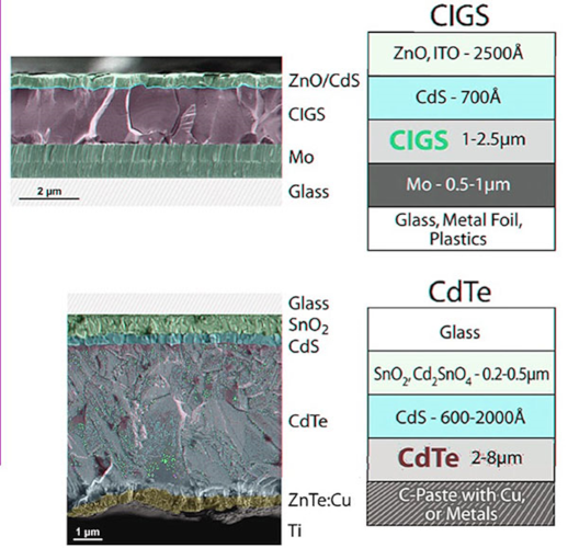
On a sectional view of the first two types of cells, obtained by electron microscopy (Figure 12), we can distinguish the different layers and the grain size.
A typical example of cells based on organic material can be seen (Figure 13).
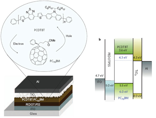
The absorber material is PCDTBT, a P-Conjugate conductive material. The junction is obtained by mixing with a material from the fullerene family, PC70BM. The carriers are extracted on the back side with a layer of nano-structured TiO2 and on the front side with another conductive material, which is covered with a transparent conductive mineral ITO layer based on tin and indium oxide.
2.3. High-efficiency multi-junction cells for space applications and concentration systems
A third family of photovoltaic cells has been developed for specific applications such as powering satellites or high-concentration terrestrial systems. These applications require cells with very high efficiency but whose cost per unit area can be high. These are multijunction cells based on so-called III-V semiconductors made of compound materials with the elements of the respective columns of the Mendeleïev table.
The active monocrystalline layers used, in which each junction is fabricated, are “heteroepitaxial” on a substrate. Epitaxy consists of depositing a layer, taking care to duplicate the crystalline arrangement of the substrate. The term heteroepitaxy is used when the chemical composition of the layer differs from that of the substrate.
This epitaxial III-V material is also used in the fabrication of light-emitting diodes, LASER diodes and many microwave devices. There is therefore a strong synergy between these different industries.
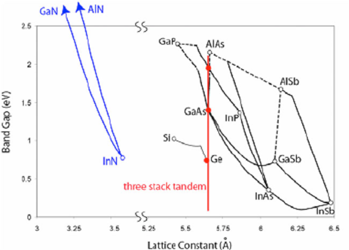
It is known that very high theoretical conversion efficiencies can be achieved by stacking several semiconductors with appropriately staggered bandgaps and electrically connecting them together. The challenge is to manufacture these materials of varying compositions with the best possible crystal quality. To achieve this, care must be taken to keep the best possible mesh agreement between the substrate and the individual layers (Figure 14).
In practice and for photovoltaic applications, a monocrystalline germanium substrate is used. This material is a semiconductor of column IV, the same as silicon, but with a lower bandgap of the order of 0.7eV.
As with silicon, massive single crystals of germanium can be fabricated using the Czochralski technique. A first junction is fabricated in this low bandgap material (0.7 eV) and then single crystal layers are grown on this substrate by epitaxy. In order to avoid dislocations detrimental to the conversion efficiency, the layer composition is adjusted to have a lattice parameter as close as possible to that of the substrate.
In III-V semiconductor materials, alloys can be obtained and the composition, and hence the band gap, can vary continuously over a certain range. Diagrams (Figure 14) show the ranges of variation of the lattice parameters and band gaps.
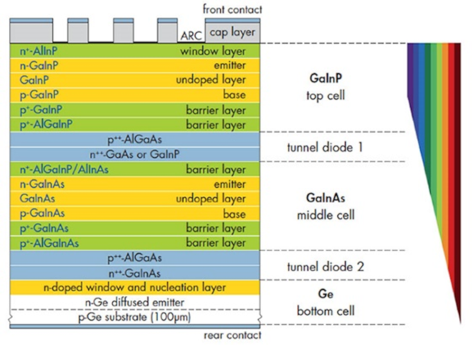
A specific example (Figure 15) shows:
- a first diode manufactured in the germanium substrate itself
- a first epitaxial layer of (GaxIn1-x) as very rich in gallium (x high and close to 1) and thus with a band gap of the order of 1.4 eV with a p-type and an n-type underlayer to fabricate the junction
- a second layer of (GaxIn1-x)P with a band gap close to 1.9 eV in which there are also n-type and p-type underlayers
At the interface between the substrate and the two layers are very thin and highly doped layers alternately of n-type and p-type, intended to facilitate the passage of electrons and thus of the electric current. These diodes are called “tunnel” diodes because the electrons can easily pass through the junction by the tunnel effect.
Each of the three junctions thus captures part of the solar spectrum (Figure 16).
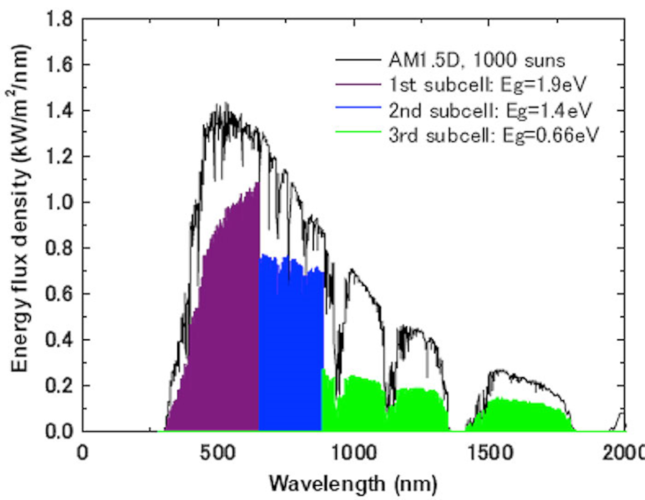
The efficiency obtained by these multijunction cells is very high, although still lower than the theoretical efficiency. It is typically in the order of 40% for the commercial cells under concentration, and goes up to 46% for the cell having obtained the absolute record under concentration and having 4 junctions [2]. These efficiencies are lower without concentration, the latter having the effect of increasing the open-circuit voltage and, consequently, the voltage at the point of maximum efficiency.
These highly efficient and sophisticated cells, given their cost and characteristics, are suitable for two types of applications.
- The space field. The cells are assembled in specific modules that are used to supply the satellites with energy. The cost of the mass put into orbit is such that the advantage of high conversion efficiency far outweighs the cost of the cells. In addition, III-V cells are much less sensitive to ionizing radiation than other cells and are therefore more reliable over time.
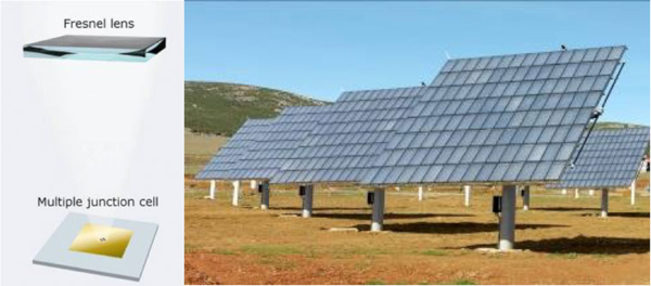
- High-concentration terrestrial photovoltaic systems (concentration factor often of the order of 400 to 500). Each cell is focused by a concentration optic, then the modules thus obtained, combining a set of optic/cell pairs, are mounted on a high-precision sun tracker. Any misalignment will lead to defocusing and loss of yield.
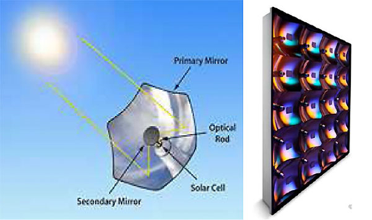
High concentration photovoltaic module technologies are illustrated by parabolic mirror reflective optics (Figure 17) and Fresnel mirror refractive optics (Figure 18).
3. Perspective of the evolution of the different PV technologies
The great diversity of photovoltaic technologies is the subject of intense development activity.
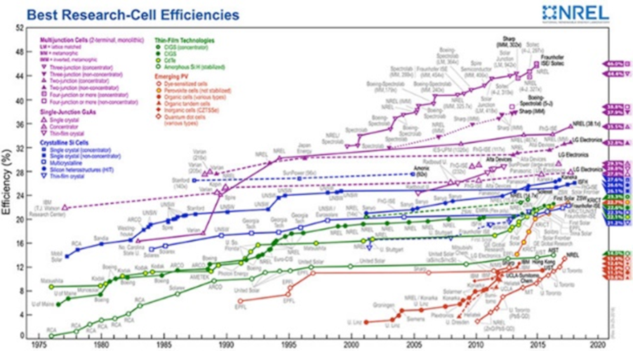
Some, such as crystalline silicon, are old. Others, such as organic cells based on pervoskites, have been introduced or discovered recently. For each technology (Figure 19), progress is constant, even for the oldest cells, whose record yields in the laboratory continue to rise. This can be seen in the graph on the US NREL website: https://www.nrel.gov/pv/assets/images/efficiency-chart.png.
It shows that progress is generally incremental and that new technologies, although they can progress quite rapidly, do not supplant older ones.
The latter technologies are approaching their theoretical maximum efficiency (30% for single-junction cells). Only mutijunction technologies, and only those based on III-V materials, exceed the 30% mark. Their industrial exploitation therefore depends on factors other than yield, such as the maturity of the technologies used, the manufacturing cost or the stability of the cells over time (Read: The evolution of costs and their springs).
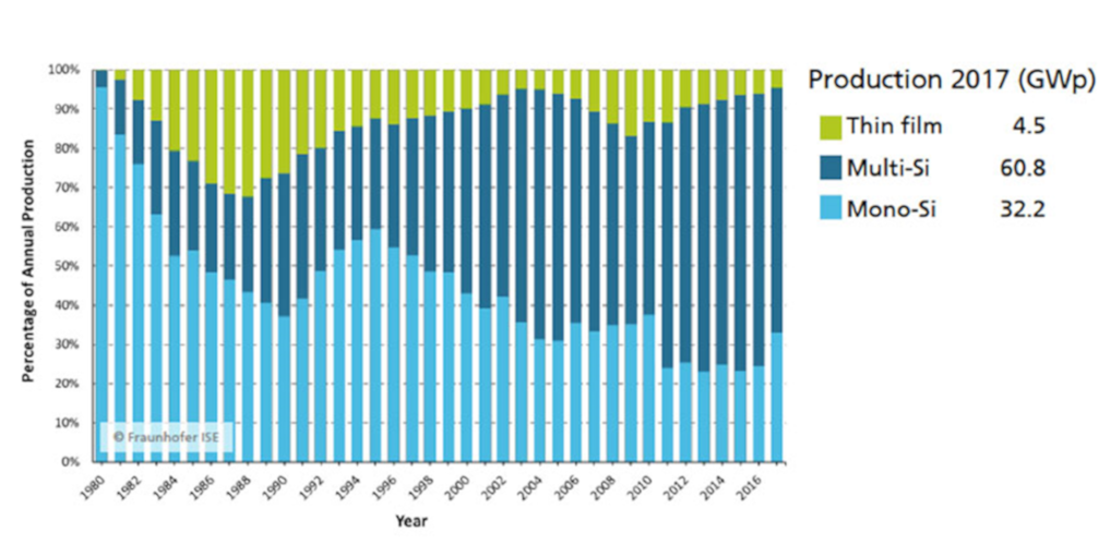
From an industrial and commercial point of view, the extreme resilience of crystalline silicon must be noted (Figure 20). Over almost four decades, its share has remained very high (never below 70%) while the market has grown by a factor of nearly 100 and continues to grow. This reveals the difficulty of supplanting a technology that is now being implemented on a very large scale, at very low cost and based on very durable products.
The share of multi-crystalline (polycrystalline) silicon has steadily increased due to its low cost per peak Watt and its relatively high yield. Use of monocrystalline silicon has recently increased due to the reduction in the share of cell price in the overall cost of systems, which favors technologies with higher efficiency. If we look at the evolution of the market share of thin films, we can see the virtual disappearance of hydrogenated amorphous silicon and the rise of CIGS at the expense of CdTe. Here again, it is the better conversion efficiency of CIGS compared to the other two, which explains why it is more resistant than CdTe and amorphous silicon in their competition with crystalline silicon. Finally, it should be pointed out that the proportion of modules based on organic materials remains almost negligible to date.
Notes and References
[1] Remember that the mm or micrometer is equal to one millionth of a meter and the nm or nanometre is equal to one billionth of a meter.
[2] F.Dimroth et al (2016). Four-Junction Wafer-Bonded Concentrator Solar Cells. IEEE, Journal of Photovoltaics, Vol. 6, No. 1, January.
L’Encyclopédie de l’Énergie est publiée par l’Association des encyclopédies de l’environnement et de l’énergie (A3E) (www.a3e.fr), contractuellement liée à l’université Grenoble Alpes et à Grenoble INP, et parrainée par l’Académie des sciences.
Pour citer cet article, merci de mentionner le nom de l’auteur, le titre de l’article et son URL sur le site de l’Encyclopédie de l’Énergie.
Les articles de l’Encyclopédie de l’Énergie sont mis à disposition selon les termes de la licence Creative Commons Attribution – Pas d’Utilisation Commerciale – Pas de Modification 4.0 International.